
Semiconductor Tools
Advanced Micro-Scale Engineering and Ultra-Pure Processing Solutions for Semiconductor Manufacturing
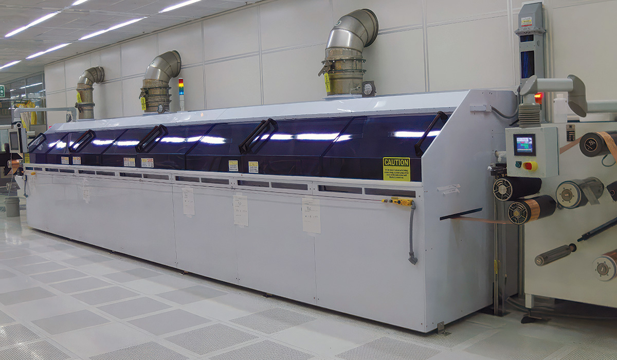

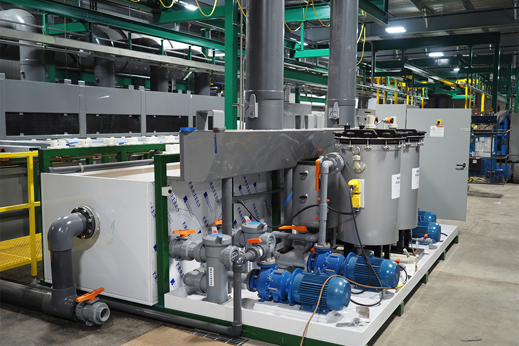
What makes our semiconductor tooling solutions truly unique is the seamless fusion of ultra-clean material compatibility, sub-micron precision fluid dynamics, and advanced contamination-free automation. Designed specifically for front-end and back-end semiconductor fabrication, advanced packaging, and microelectronic device manufacturing, our systems eliminate particle generation, drastically reduce chemical leaching, and maintain rigorous process repeatability across high-volume production cycles. By combining electrochemically pure architecture with fully synchronized cleanroom utility integration, we deliver robust, high-throughput manufacturing assets built to withstand aggressive semiconductor chemistries while maximizing your wafer yield and operational uptime.
Building a high-reliability semiconductor processing tool requires the absolute mastery of ultra-pure fluid delivery, contamination control, and sub-micron positioning accuracy. Every semiconductor system we construct follows a rigorous, end-to-end execution framework tailored specifically to your facility’s cleanroom and production demands—transforming complex micro-scale finishing requirements into a robust, high-throughput manufacturing asset built for maximum uptime and zero-defect yield.
We begin by optimizing every wet bench, process tank, fluid manifold, and wafer-handling assembly for extreme chemical purity and mechanical durability. Leveraging advanced automation logic and ultra-clean architectural design, we engineer scalable semiconductor tools engineered to maintain flawless particulate control at high production speeds while integrating cleanly with your plant’s existing facilities.
Our multidisciplinary engineering team collaborates across mechanical, electrical, chemical, and control disciplines to design your semiconductor processing equipment around your exact cleanroom workflow. Every chemical etch station, rinsing module, automated wafer transfer mechanism, and megasonic cleaning tank is custom-configured to optimize process flow for advanced packaging, silicon processing, and substrate manufacturing.
We unify complex operational streams—such as specialized ultra-pure water (UPW) loops, localized exhaust scrubbers, chemical delivery systems, and cleanroom HVAC infrastructure—into a single, coordinated plant architecture. From detailed electrical schematics to comprehensive PLC and HMI programming, we ensure total regulatory compliance, particle containment, and smooth data connectivity across your entire microelectronic fabrication ecosystem.
Every build moves forward with absolute transparency, structured organization, and active collaboration. Through disciplined project tracking, scheduled design reviews, and clear milestone management, we maintain strict quality control and keep your teams completely aligned from initial blueprint to final delivery.
Our seasoned field technicians manage complete cleanroom installation, fluid calibration, and electrical integration to ensure every element meets rigorous semiconductor design specifications. Each bath, robot, and control panel is particle-checked, fine-tuned, and paired with hands-on operator training to guarantee immediate production readiness.
We unite engineering accuracy with practical cleanroom execution through thorough structural and utility validation. Overseeing every phase up to final turnover, we ensure your new semiconductor processing tool reaches full production capacity rapidly, backed by verified performance data and long-term lifecycle support.
Executing a high-precision semiconductor tooling project demands an uncompromising standard of technical accuracy and particulate control. Our comprehensive four-stage framework systematically governs every phase of development—from initial blueprinting and ultra-pure material selection to intelligent automation integration and rigorous cleanroom commissioning—ensuring absolute synchronization across mechanical, chemical, and control architectures to maximize your wafer yield, eliminate contamination risks, and safeguard long-term operational reliability.
Our mechanical, electrical, chemical, and software engineers collaborate directly to master the physics of sub-micron wet processing and wafer handling. By deeply understanding ultra-pure fluid dynamics, chemical etch rates, and cleanroom particulate dynamics, our team designs robust architectures engineered specifically to prevent contamination, optimize chemical usage, and maximize throughput.
We construct every semiconductor component—from PVDF/PTFE process tanks and megasonic arrays to automated wafer transfer robots and chemical recovery loops—tailored precisely to your cleanroom footprint and production goals. Using electrochemically inert, ultra-pure materials, our custom equipment is built to withstand continuous exposure to aggressive semiconductor chemistries.
We unify your semiconductor processing tools with advanced automation and control systems, linking closed-loop chemical dosing pumps, programmable logic controllers, and HMI touchscreens directly to your facility’s UPW, exhaust, and waste neutralization streams for seamless data connectivity and compliance.
We ensure long-term operational success through rigorous on-site particulate testing, comprehensive documentation, and hands-on operator training. Every system is thoroughly validated for etch uniformity, rinse efficiency, and mechanical stability before handoff, backed by ongoing lifecycle support to protect your investment.
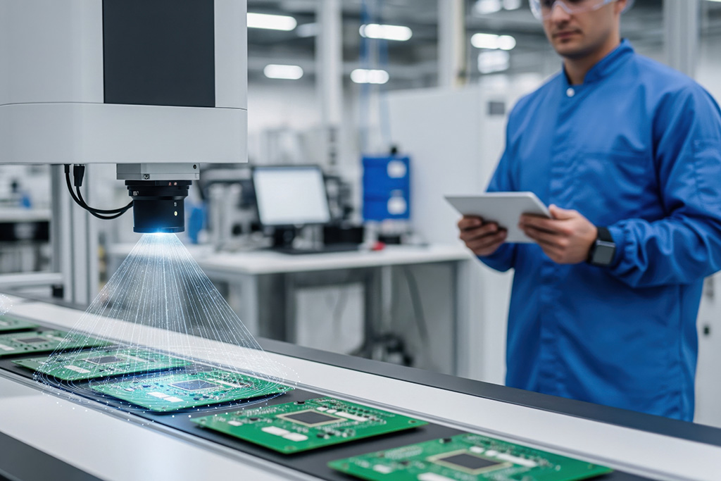
A Tier-1 semiconductor manufacturer supplying advanced microelectronic components for high-reliability computing applications was facing persistent yield and particulate bottlenecks using legacy wet processing benches. Their older equipment struggled with chemical bath degradation, uneven etch rates across 300mm substrates, and high particle counts generated by aging mechanical transfer mechanisms. Needing to scale capacity without compromising strict cleanroom particle standards or wafer-to-wafer repeatability, the facility partnered with Precision Process to engineer and commission a heavy-duty, ultra-pure automated semiconductor processing tool.
Precision Process deployed a custom-tailored wet processing system featuring high-purity PVDF construction, closed-loop megasonic agitation, automated robotic wafer handling with zero-particulate tracking, and multi-stage cascading ultra-pure water rinse stations. The new system integrated seamlessly with the plant’s existing central UPW loop, exhaust scrubbers, and chemical waste neutralization infrastructure.
Within the first quarter of operation, the facility achieved a 35% reduction in particle-induced wafer defects, a dramatic improvement in etch uniformity across all processed substrates, and zero unscheduled downtime across continuous cleanroom shifts.
Director of Manufacturing Operations
Navigate this focused resource to explore how Precision Process resolves the primary mechanical, chemical, and particulate challenges inherent in semiconductor wet processing. From engineering ultra-pure fluid dynamics to eliminate contamination and deploying automated wafer-handling systems to ensure sub-micron precision, these engineering-driven solutions demonstrate how our custom semiconductor tools safeguard your facility’s production yield, maintain strict cleanroom compliance, and ensure uncompromised uptime across continuous operating cycles.
Particulate generation and chemical extractables destroy microelectronic yields. Precision Process addresses this by constructing all process tanks, piping manifolds, and structural enclosures from electrochemically inert, ultra-pure materials like PVDF, PFA, and specialized stainless steels. Systems are designed with smooth internal radii, zero dead-leg fluid paths, and isolated mechanical drives to ensure absolute particulate containment and cleanroom compatibility.
High-purity water usage and chemical waste disposal represent massive operating costs in semiconductor fabrication. Our systems utilize optimized cascading counter-current rinse tanks, high-efficiency spray-under-immersion modules, and closed-loop chemical recovery loops. This engineered isolation captures valuable process solutions and minimizes UPW consumption without compromising rinse cleanliness.
Aggressive acids, strong bases, and continuous exposure to ultra-pure water rapidly degrade standard equipment frames and motion components. Precision Process combats this by isolating all drive mechanisms and robotic actuators outside the process zone, shielding them from chemical vapors and utilizing sealed, corrosion-resistant components designed for long operational lifecycles.
Semiconductor fabrication equipment cannot operate effectively as an isolated island; it requires synchronized facility exhaust, continuous ultra-pure water supply, and dedicated chemical drain segregation. Our engineering methodology unifies auxiliary utilities into the core design phase. We map out centralized fume scrubbers, UPW loops, and automated chemical discharge streams alongside precise electrical and PLC schematics, ensuring your new tool connects cleanly to your existing facility infrastructure without compliance gaps.
Unscheduled downtime in a semiconductor fab halts entire production lots and results in severe financial losses. We minimize operational risk by utilizing modular component architectures, heavy-duty structural assemblies, and intuitive HMI diagnostic controls that alert maintenance teams to pressure anomalies, flow restrictions, or mechanical wear before failures occur. Furthermore, our field technicians provide rigorous cleanroom calibration and hands-on operator training during startup to ensure peak mechanical reliability from day one.
Collaborate directly with our engineering team to map out the ideal course of action for your facility, ensuring every detail of your custom semiconductor processing tool is optimized for your exact workflow, throughput goals, and long-term operational success.